Видео с ютуба And Gate Schematic
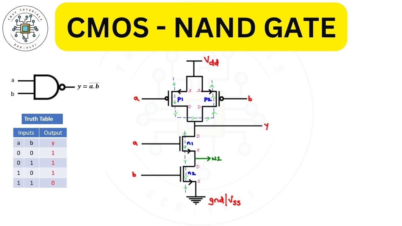
CMOS NAND Gate Schematic Explained | Transistor-Level Design, Working & Simulation in VLSI
Making logic gates from transistors

Understanding Logic Gates

9. Drawing the schematic and icon of a NAND gate

Diode Logic Gates - OR, NOR, AND, & NAND

Design of AND Gate Schematic in Cadence Virtuoso #cadence #virtuoso #vlsi #vlsidesign

CMOS Logic Gates Explained | Logic Gate Implementation using CMOS logic

Transistor Logic Gates - NAND, AND, OR, NOR

Logic Gates, Truth Tables, Boolean Algebra AND, OR, NOT, NAND & NOR
![Logic Gates :- AND Gate [ Theory + Practical + Application ] (In Hindi)](https://imager.clipsaver.ru/LBuLmC0chyQ/max.jpg)
Logic Gates :- AND Gate [ Theory + Practical + Application ] (In Hindi)

Kicad Tutorial 29 : Design and Simulation of AND gate circuit and verifying the AND gate truth table

Цифровая электроника: логические вентили – интегральные схемы. Часть 1

Design of OR Gate Schematic in Cadence Virtuoso #cadence #virtuoso #vlsi #vlsidesign

Design of 3 input AND Gate Schematic in Cadence Virtuoso #cadence #virtuoso #vlsi #vlsidesign

Cadence Virtuoso:: Design of NAND Gate Schematic || Part-1.

AND Gate Schematic in Cadence Virtuoso || Logic Gates - AND Gate

Backend Lab 5: XOR Gate Schematic

Digital Logic Gates from Transistors, AND, NAND, OR, NOR, XOR, XNOR, Buffer, and Inverter

Stick diagram of CMOS AND gate

Electronics #2 AND Gate Switching Circuit TUTORIAL

How Logic Gates Work - The Learning Circuit

Electronics #3 OR Gate Switching Circuit TUTORIAL

Schematic diagram and layout of two input NOR gate

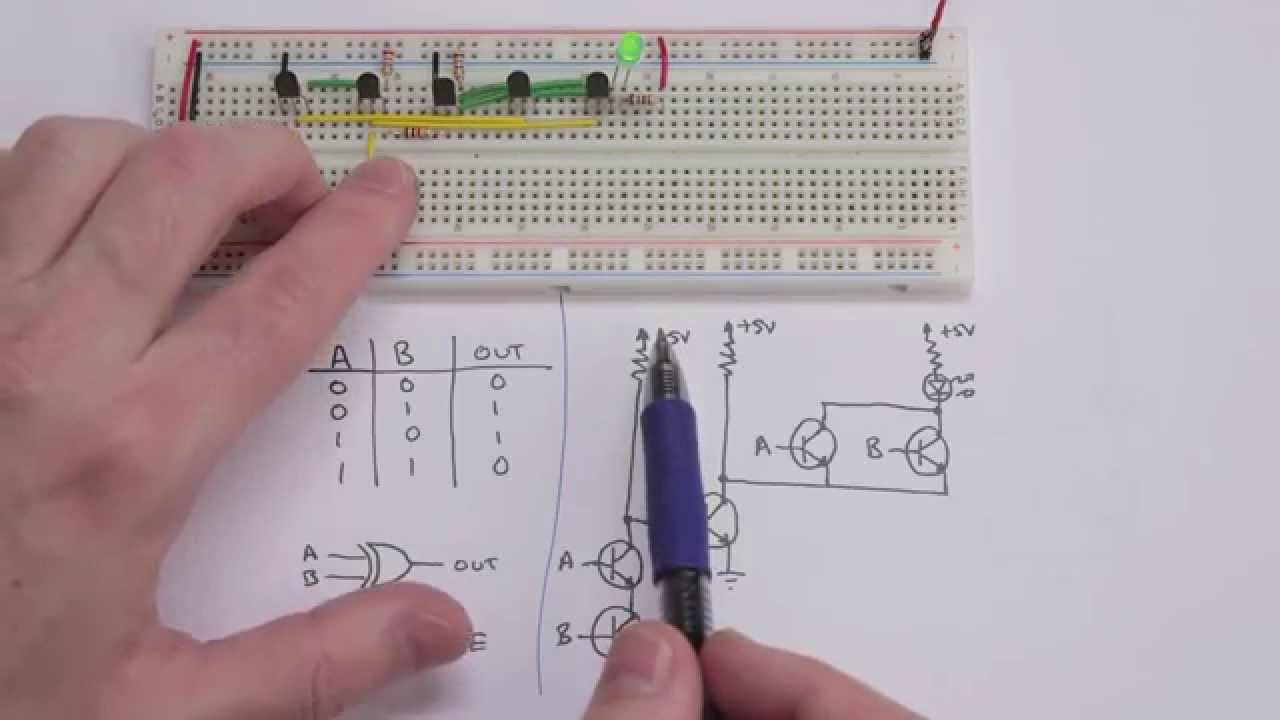
EX-OR Gate - Circuit Diagram and Truth Table - Logic Gates - Application of Electronics Class 12